Microcontroller architecture
Introduced| English | Meaning |
|---|---|
| microcontroller | A small computer on one chip, with processor, memory and input/output, built to control a device. |
| bus/bʌs/ | A shared set of wires that carries data, addresses or control signals between parts of a computer. |
| fetch-decode-execute cycle | The processor sequence of obtaining an instruction, interpreting it and carrying it out. |
| program counter/ˈprəʊɡræm ˈkaʊntə/ | The register that holds the address of the next instruction to fetch. |
| clock/klɒk/ | A regular square-wave signal that tells a digital circuit when to update. |
| memory map | memory map |
A computer the size of a grain of rice
- A thermostat, an anti-lock brake controller and a wireless earbud each contain a complete computer on one tiny chip, costing less than the postage to ship it.
- This lesson opens that chip: what is inside, how it runs a program, and how fast.
Three parts on one chip
- A microcontroller 微控制器 puts flash memory (the program), SRAM (the data) and a CPU on one chip, together with peripherals for the outside world.
- Every transfer between them travels on a bus 总线: address lines say where, data lines carry what, control lines say read or write.
Match each part of a microcontroller to what it holds or does.
Difficulty 2/5 · 140 coins + a small bonus on first completion today
All four sit on one chip, which is what makes a microcontroller cheap and small.
Fetch, decode, execute
- The CPU repeats the fetch-decode-execute cycle 取指译码执行周期. The program counter 程序计数器 (PC) holds the address of the next instruction; the CPU fetches it, decodes it and executes it.
- Then the PC moves on, or jumps for a branch. The clock 时钟 paces every step.
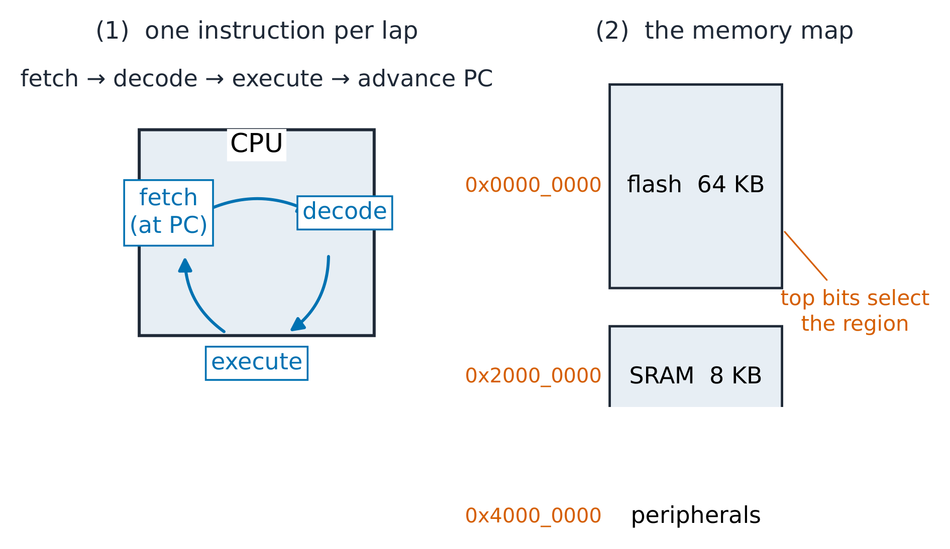
Put one instruction's cycle in order.
Difficulty 3/5 · 200 coins + a small bonus on first completion today
The cycle then repeats at the new PC value, once per instruction.
The memory map
- An $N$-bit address reaches $2^{N}$ locations, so a memory of a given size needs $N = \log_{2}(\text{size})$ address lines.
- Each region of the memory map 存储器映射 sits at its own base address. Regions whose top address bits differ can never overlap.
Flash at 0x0000_0000 and SRAM at 0x2000_0000 can overlap if the flash is large enough.
Difficulty 1/5 · 100 coins + a small bonus on first completion today
The regions differ in their top address bits, so no address can belong to both; the decoder separates them by those bits.
Worked example: sizing the map
- 64 KB of flash is $2^{16}$ bytes: 16 address lines, from
0x0000_0000to0x0000_FFFF. - 8 KB of SRAM is $2^{13}$ bytes: 13 lines, from
0x2000_0000to0x2000_1FFF. The top bits differ, so the two can never collide.
Which byte does this address select?
$address=base+offset,\quad N=\lceil\log_2(size\ in\ bytes)\rceil$
Compare the worked 64 KiB flash and 8 KiB SRAM regions. Move from the last mapped byte to the next address, separate the base from the offset bits, and explore why 96 KiB needs 17 offset bits but leaves 32 KiB unused in its address window.
8 KB of SRAM needs how many address lines?
Difficulty 1/5 · 100 coins + a small bonus on first completion today
$8\,\text{KB} = 8192 = 2^{13}$ bytes, so 13 lines; it spans 0x2000_0000 to 0x2000_1FFF.
32 KB of flash starts at address 0. What is its last address, in decimal?
Difficulty 2/5 · 140 coins + a small bonus on first completion today
$32\,\text{KB} = 32\,768$ bytes, numbered 0 to 32 767, which is 0x7FFF.
Worked example: the time per instruction
- At 84 MHz and about one instruction per cycle, one instruction takes $\dfrac{1}{84 \times 10^{6}} = 11.9\,\text{ns}$.
- A 100-instruction control pass takes 1.19 µs, so a 1 ms control period has room for about 840 such passes. This budget arithmetic returns in every later lesson.
At 84 MHz, one instruction per cycle, a 100-instruction routine takes about
Difficulty 1/5 · 100 coins + a small bonus on first completion today
$100 \times 11.9\,\text{ns} = 1.19\,\mu$s.
Three common slips
- Address lines for data width. Address lines count locations; data lines set how wide each one is.
- Bits for bytes. Flash is sized in bytes; mixing them is a factor of eight.
- Assuming a boot address. The vendor fixes the map; the linker script must match it.
A 48 MHz CPU runs a 240-instruction control routine (one instruction per cycle). How many times can it run per millisecond?
Difficulty 2/5 · 140 coins + a small bonus on first completion today
$48\,000$ cycles per millisecond divided by 240 cycles per run gives 200 runs.
Recap
- Flash, SRAM and CPU on one chip, joined by the bus and paced by the clock.
- Fetch, decode, execute, advance the PC; repeat.
- $N$ address lines reach $2^{N}$ bytes; the clock turns instruction counts into time.